

Photovoltaic cells convert sunlight directly into electricity through the photovoltaic effect, a quantum mechanical process in which photons knock electrons loose from atoms in semiconductor materials, generating an electric current. This technology forms the foundation of modern solar energy systems, transforming how we harvest power from the sun without moving parts, fuel, or emissions.
Understanding how photovoltaic cells work matters for anyone evaluating solar technology, whether you’re considering rooftop panels, studying renewable energy systems, or simply curious about the science behind the global shift toward sustainable electricity generation. The mechanism itself is elegant: specialized materials arranged in precise layers create an electric field that channels freed electrons into a usable current. What appears simple from the outside involves careful engineering of semiconductor properties, surface treatments, and electrical contacts that determine how efficiently light becomes power.
Different types of photovoltaic cells achieve this conversion through varying approaches. Silicon-based technologies dominate the market but compete with thin-film alternatives, emerging perovskite designs, and multi-junction cells that layer materials to capture different wavelengths of light. Each type balances efficiency, cost, durability, and manufacturing complexity differently, making the choice of cell technology context-dependent rather than universal.
This article explains the step-by-step process occurring inside a photovoltaic cell when sunlight strikes its surface, breaks down the key components that enable this energy transformation, and compares how different cell technologies execute the same fundamental principle with distinct material strategies and performance characteristics. By the end, you’ll grasp both the physics driving solar electricity generation and the practical differences that distinguish one photovoltaic technology from another.
What Photovoltaic Cells Are
Photovoltaic cells are semiconductor devices that transform light energy directly into electrical energy through a phenomenon called the photovoltaic effect. Unlike engines or turbines that convert fuel or motion into power, these cells generate electricity with no moving parts, no combustion, and no noise, just the interaction between sunlight and specially prepared materials.
At their core, photovoltaic cells exploit the behaviour of semiconductors, materials that sit between conductors and insulators in their ability to carry electrical current. When light strikes a photovoltaic cell, it doesn’t simply heat the material. Instead, particles of light called photons transfer their energy to electrons within the semiconductor, knocking them loose from their atomic bonds and allowing them to flow as electrical current.
Understanding a few key terms helps clarify how this process works:
- Photovoltaic effect
- The generation of electric current when certain materials absorb light energy. This effect, discovered in 1839, forms the basis for all solar cell operation.
- Semiconductor
- A material (typically silicon) whose electrical conductivity falls between that of a conductor and an insulator. Semiconductors can be modified to control how electrons move through them.
- Photon
- A particle of light that carries energy. When photons strike a solar cell with sufficient energy, they can free electrons from atoms in the semiconductor material.
- Electron-hole pair
- The free electron and the vacant space (hole) it leaves behind when knocked loose by a photon. Both particles contribute to electrical current in opposite directions.
- P-N junction
- The boundary between two types of semiconductor material (p-type and n-type) that creates an internal electric field. This junction separates charge carriers and drives current flow.
The beauty of photovoltaic cells lies in their elegant simplicity. They contain no fuel to burn, no fluids to circulate, and no mechanical components to wear out. A typical cell consists of thin layers of semiconductor material, metal contacts to collect the generated electricity, and an anti-reflective coating to maximize light absorption. When assembled into panels and connected to an electrical circuit, these cells provide a silent, clean power source that works anywhere the sun shines.
How Photovoltaic Cells Work

The Photovoltaic Effect
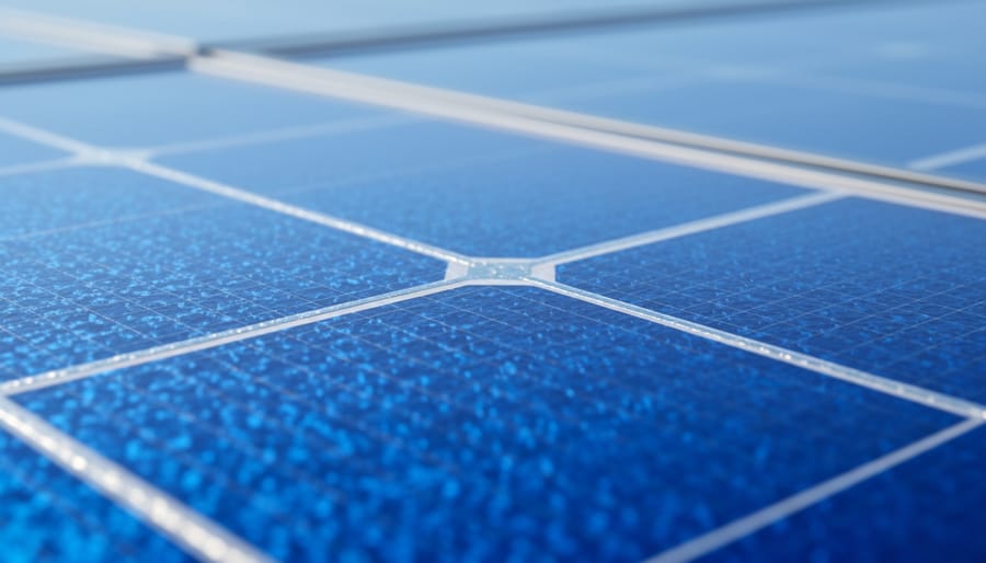
The photovoltaic effect begins the moment a photon, a particle of light, strikes the surface of a semiconductor material, typically silicon. When that photon carries sufficient energy, it transfers that energy to an electron bound within the silicon’s atomic structure. This energy boost frees the electron from its usual position, creating what physicists call an electron-hole pair.
Think of it like a crowded theater where everyone occupies a seat. When someone (an electron) stands up and leaves, they create both a moving person and an empty seat behind them. In semiconductors, the “empty seat” left behind, the hole, behaves like a positive charge that can also move through the material.
Not every photon succeeds in this process. The photon must carry enough energy to overcome what’s called the bandgap, an energy threshold specific to each semiconductor material. Silicon’s bandgap requires photons from visible and near-infrared light. Photons with too little energy pass through harmlessly, while those with excess energy create heat alongside the electron-hole pair.
This electron liberation happens countless times per second across millions of atoms when sunlight bathes a solar cell. Each freed electron potentially contributes to electrical current, but without additional structure, these electrons and holes would simply recombine within nanoseconds, releasing the absorbed energy as heat rather than electricity. The p-n junction solves this problem by separating the charges before they reunite.
The Role of the P-N Junction
At the heart of every photovoltaic cell sits a p-n junction, the crucial boundary that transforms excited electrons into usable electrical current. Without this engineered structure, electrons freed by incoming photons would simply recombine with holes before any electricity could flow.
The junction forms where two specially treated silicon layers meet. Through a process called doping, manufacturers introduce controlled impurities into pure silicon to create distinct electrical properties. N-type silicon contains extra electrons (added by doping with phosphorus or arsenic), while p-type silicon has a deficit of electrons, creating positively charged “holes” (achieved by doping with boron or gallium). These holes act as mobile positive charges that electrons can fill.
When these two layers join, something remarkable happens at their interface. Electrons from the n-type region diffuse across to fill holes in the p-type region, while holes migrate the opposite direction. This movement creates a depletion zone at the junction, a thin region depleted of mobile charge carriers. More importantly, this charge migration establishes a permanent electric field pointing from the n-type side toward the p-type side.
This built-in electric field acts as a one-way gate for charge carriers. When photons strike the cell and create electron-hole pairs, the field immediately separates them before they can recombine. It pushes electrons toward the n-type layer (which becomes the negative terminal) and holes toward the p-type layer (the positive terminal). This enforced separation maintains a voltage difference between the two sides of the cell.
Connect these terminals through an external circuit, and the separated charges flow as electrical current, driven by the voltage the junction creates. The p-n junction essentially converts random electron motion into directed flow.
From Sunlight to Electricity
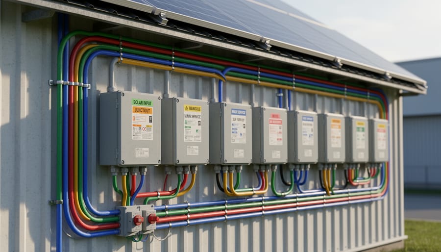
Once photons dislodge electrons at the p-n junction, those liberated charge carriers must travel through a complete circuit to become usable electricity. The electron flow follows a carefully engineered pathway from the semiconductor material through external connections and back again.
Electrons freed in the n-type layer migrate toward metal contacts positioned on the cell’s front surface. These contacts form a collection grid, thin metallic fingers that spread across the cell face like a web, capturing electrons while minimizing shading of the active semiconductor area. The grid design balances two competing needs: sufficient coverage to collect current efficiently and minimal obstruction of incoming sunlight. Engineers typically configure these fingers to feed into larger bus bars that channel electrons toward the cell’s edge.
From the front contacts, electrons flow through external wiring to power a load, perhaps a battery, an appliance, or a solar power system connected to the grid. As electrons work their way through this circuit, they deliver energy to whatever device needs electricity. The current then returns to the photovoltaic cell through a back contact, usually a continuous metal layer covering the entire rear surface.
Returning electrons re-enter the p-type semiconductor layer, where they recombine with the holes left behind when electrons initially jumped to the n-type side. This recombination completes the circuit. As long as photons continue striking the cell, the process repeats continuously: absorption creates electron-hole pairs, the junction separates them, contacts collect the charge carriers, and the external circuit harnesses their movement as direct current electricity.
Types of Photovoltaic Cells
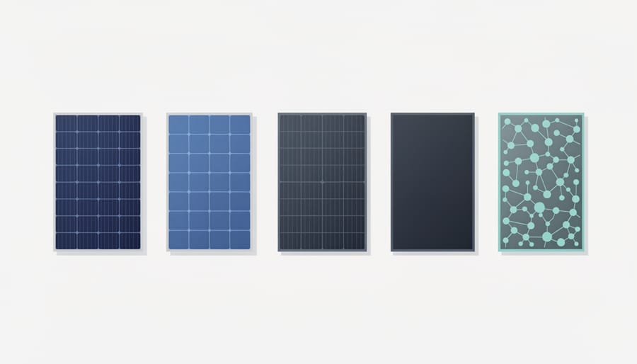
Monocrystalline Silicon Cells
Monocrystalline silicon cells represent the most efficient commercially available photovoltaic technology, manufactured from single, continuous crystal structures of pure silicon. During production, a cylindrical ingot grows from a silicon seed crystal through the Czochralski process, then gets sliced into thin wafers. This single-crystal structure allows electrons to move more freely with fewer defects or boundaries interrupting their path, directly translating to superior electrical performance.
You’ll recognize monocrystalline cells by their distinctive uniform black or deep blue appearance and rounded edges where circular wafers were trimmed to fit rectangular panels. The consistent crystal lattice enables these cells to convert 22-27% of incoming sunlight into electricity under standard test conditions, with laboratory prototypes achieving even higher rates according to the NLR research-cell efficiency chart. This efficiency advantage means a smaller array generates the same power output as larger systems using less efficient technologies.
The precision manufacturing and high-purity silicon required make monocrystalline cells the premium-priced option in the photovoltaic market. Despite the higher upfront cost, they’re the optimal choice for space-constrained residential rooftops, urban installations, and any application where maximizing power output per square metre justifies the investment. Their superior performance in low-light conditions and better temperature coefficients also make them advantageous in less-than-ideal climates.
Polycrystalline Silicon Cells
Polycrystalline silicon cells are manufactured by melting multiple silicon fragments together and cooling them into ingots, which are then sliced into wafers. This process creates a multi-crystal structure where numerous individual silicon crystals meet at grain boundaries, giving these cells their distinctive blue speckled appearance. Unlike the uniform surface of monocrystalline cells, the varied crystalline structure reflects light differently across the wafer.
The manufacturing method makes polycrystalline cells less expensive to produce than their monocrystalline counterparts. Melting and casting silicon requires less energy and generates less waste material, reducing overall production costs by approximately 20-30%. However, this affordability comes with a trade-off in performance. The grain boundaries between crystals create resistance that impedes electron flow, limiting efficiency to 17-22% compared to monocrystalline cells.
These cells work best for projects where space constraints aren’t critical and budget considerations take priority. Residential installations with ample roof area, ground-mounted arrays, and large commercial solar farms commonly use polycrystalline panels to maximize cost-effectiveness. While you’ll need more panel area to generate the same power output as monocrystalline systems, the lower upfront investment often makes polycrystalline technology the practical choice for cost-sensitive applications.
Thin-Film Cells
Thin-film cells take a fundamentally different approach from crystalline silicon technologies. Instead of cutting wafers from solid crystal ingots, manufacturers deposit extremely thin layers of photovoltaic material, often just micrometers thick, onto substrates like glass, metal, or flexible plastic. This manufacturing method reduces material costs and opens possibilities for applications where traditional rigid panels won’t work.
The three main thin-film variants rely on different semiconductor compounds. Cadmium telluride (CdTe) cells dominate commercial thin-film production, offering reasonable efficiency (around 16-18%) at low manufacturing cost. Amorphous silicon (a-Si) uses non-crystalline silicon in ultra-thin layers, achieving 6-10% efficiency but excelling in low-light conditions. CIGS cells (copper indium gallium selenide) represent the efficiency leader among thin films, reaching 15-20% while maintaining the technology’s inherent advantages.
The thin-film solar cell flexibility makes these technologies valuable for specialized applications. Lightweight flexible versions conform to curved surfaces on vehicles, portable devices, and building facades where conventional panels can’t mount. Their lower efficiency per square meter means they need more installation area than crystalline options for equivalent power output.
Thin-film cells also perform relatively better in high temperatures and partial shading compared to crystalline silicon. These characteristics make them suitable for large-scale utility installations in hot climates, building-integrated photovoltaics, and consumer products where weight, flexibility, or manufacturing cost outweigh peak efficiency concerns.
Perovskite Cells
Perovskite cells represent one of the most promising developments in photovoltaic technology. These cells use perovskite-structured materials, typically hybrid organic-inorganic compounds like methylammonium lead halides, as the light-absorbing layer. Their name comes from the crystal structure, which mimics that of the mineral perovskite.
What sets perovskite cells apart is their manufacturing process. Researchers can deposit the active material from solution using simple techniques like spin-coating or inkjet printing, drastically reducing production costs compared to traditional silicon processing. This approach requires far less energy and fewer specialized facilities.
Efficiency has climbed remarkably fast. Laboratory perovskite cells now exceed 25% efficiency, rivaling established silicon technology after only a decade of intensive research. Some tandem designs that stack perovskite layers atop silicon cells have pushed beyond 30% efficiency.
However, stability remains the critical challenge preventing widespread commercial deployment. Perovskite materials degrade when exposed to moisture, heat, and ultraviolet light. Current cells can lose performance after months of outdoor exposure, falling short of the 25-year lifespan standard for solar panels.
Researchers are developing encapsulation techniques and more stable perovskite compositions to address these durability issues. If stability improves, perovskite cells could enable lightweight, flexible solar applications and dramatically lower the cost of photovoltaic energy.
Multi-Junction and Concentrator Cells
Multi-junction cells represent the cutting edge of photovoltaic efficiency by stacking multiple semiconductor layers, each tuned to absorb a different portion of the light spectrum. Where conventional single-junction cells capture only a narrow band of wavelengths efficiently, multi-junction designs use materials like gallium arsenide, indium gallium phosphide, and germanium arranged in a vertical stack. Photons pass through the top layer, which absorbs high-energy blue light, then continue to deeper layers optimized for green, red, and infrared wavelengths. This cascading approach captures far more of the sun’s energy, routinely achieving efficiencies exceeding 40% in laboratory conditions and above 35% in commercial products.
These cells power virtually all satellites and spacecraft, where weight constraints and limited surface area make their high cost per watt worthwhile. On Earth, concentrator photovoltaic systems use lenses or mirrors to focus sunlight hundreds of times onto small multi-junction cells, dramatically reducing the expensive semiconductor area needed while maintaining high output. However, concentrator systems require precise sun-tracking mechanisms and perform poorly in diffuse or cloudy light, limiting deployment to regions with strong direct sunlight like desert installations. The complexity and expense keep multi-junction technology confined to specialized applications where maximum efficiency justifies the premium.
Where Photovoltaic Cells Are Used
Photovoltaic cells power an expanding range of applications worldwide, with specific cell technologies chosen to match performance requirements, space constraints, and economic considerations in each sector.
Residential installations represent the most visible application, where homeowners mount solar panels on rooftops to reduce electricity bills and carbon footprints. Monocrystalline cells dominate this market due to their high efficiency, which maximizes power generation on limited roof space. Grid-connected systems feed excess electricity back to utility networks, while battery-coupled systems provide backup power during outages. In remote areas without grid access, off-grid photovoltaic systems paired with battery storage deliver reliable electricity for lighting, refrigeration, and communication devices.
Commercial and industrial facilities deploy large-scale photovoltaic arrays on warehouse roofs, parking structures, and adjacent land to offset significant energy consumption. These installations often use polycrystalline cells, which offer a favorable balance between efficiency and cost for larger available areas. Thin-film technologies find applications where lightweight, flexible panels suit curved surfaces or portable power needs.
Utility-scale solar farms generate hundreds of megawatts using vast arrays of photovoltaic modules that feed electricity directly into transmission grids. These facilities typically deploy the most cost-effective technology per watt generated, with site-specific factors like available land area and solar irradiance influencing cell type selection. Concentrator photovoltaic systems using multi-junction cells operate in regions with high direct sunlight, achieving record conversion efficiencies through optical concentration.
Beyond terrestrial applications, photovoltaic cells serve critical roles in:
- Space satellites and probes, where multi-junction cells provide maximum power from minimal panel area in the harsh space environment
- Portable consumer electronics like calculators, phone chargers, and camping equipment using small amorphous silicon or crystalline panels
- Solar-powered vehicles including experimental aircraft, boats, and electric vehicle range extenders
- Building facades and windows incorporating integrated photovoltaics that serve both architectural and power-generation functions
- Agricultural applications powering irrigation systems, electric fencing, and greenhouse operations in remote farming areas
- Emergency and disaster relief operations where portable solar generators provide immediate power restoration
- Traffic infrastructure including solar-powered road signs, streetlights, and parking meters eliminating costly grid connections
The versatility of photovoltaic technology continues expanding as cell efficiencies improve and costs decline, making solar electricity practical for an ever-broadening spectrum of energy needs across developed and developing nations alike.
Common Questions About Photovoltaic Cells
Photovoltaic cells have transformed how we generate electricity, but their operation and performance raise practical questions for anyone considering solar technology. Understanding efficiency factors, durability, and environmental considerations helps you make informed decisions about solar adoption.
What affects photovoltaic cell efficiency?
Cell efficiency depends on material purity, temperature (performance drops in extreme heat), light intensity, angle of sunlight, and semiconductor type. Shading, dirt accumulation, and age also reduce conversion rates over time.
How long do photovoltaic cells last?
Most silicon-based cells maintain 80-85% of their original efficiency after 25-30 years. Manufacturers typically guarantee performance for 25 years, though cells often continue generating electricity beyond this warranty period at gradually declining rates.
Do photovoltaic cells work on cloudy days?
Yes, but at reduced capacity. Cells generate 10-25% of their rated output on heavily overcast days since diffuse sunlight still contains photons that excite electrons in the semiconductor material.
Can photovoltaic cells be recycled?
Silicon cells are recyclable, with glass, aluminum frames, and semiconductor materials recoverable through specialized processes. Growing recycling infrastructure addresses end-of-life concerns, particularly important as early installations reach retirement age.
Efficiency improvements continue as researchers refine manufacturing techniques and explore new materials. Perovskite cells show particular promise, with laboratory efficiencies climbing rapidly while production costs fall. Tandem architectures that layer different semiconductors could push practical efficiencies beyond 30% in coming years, making solar competitive in even more applications.
Environmental considerations extend beyond individual cells to large-scale deployments. Questions about land use, habitat disruption, and ecosystem impacts matter when evaluating the solar farms environment footprint. Research continues to balance renewable energy expansion with ecological stewardship, ensuring that photovoltaic technology delivers genuine sustainability benefits across its entire lifecycle.
Photovoltaic cells transform sunlight into electricity by harnessing the photovoltaic effect within semiconductor materials. When photons strike the p-n junction, they excite electrons, generating a flow of direct current that powers homes, businesses, and entire grids. This elegant physics underpins a technology that has become central to global energy strategies.
Understanding the distinctions between monocrystalline, polycrystalline, thin-film, perovskite, and multi-junction cells equips decision-makers to match technology with context. A homeowner maximizing rooftop output selects high-efficiency monocrystalline panels. A large-scale utility project in a sun-drenched region might favor cost-effective polycrystalline arrays. Emerging perovskite research promises lighter, flexible alternatives that could expand solar’s reach into new applications.
The stakes extend beyond technical specifications. Photovoltaic deployment directly addresses the air pollution connection by displacing fossil fuel combustion, while driving improvements in energy efficiency across entire power systems. As manufacturing scales and performance improves, solar becomes more accessible to communities worldwide.
Grasping how photovoltaic cells work, from photon absorption to electron flow, empowers you to evaluate claims, compare products, and participate meaningfully in discussions about renewable energy. That informed engagement accelerates the transition to sustainable systems that benefit everyone.